
Technology
YouTuber's backyard fab ambitions expand from RAM to homebrew LEDs
Key Points
A YouTuber on a mission to liberate semiconductor manufacturing from the grip of multinational megacorporations is back with a new round of DIY success, this time manufacturing working LEDs in his backyard fab. Dr. Semiconductor, also known as semiconductor engineer Dr. Matthew Hartensveld, per his recently launched website, first caught the internet’s attention five months ago when he built a class-100 cleanroom in a shed in his backyard. Back in April, we wrote about his successful project...
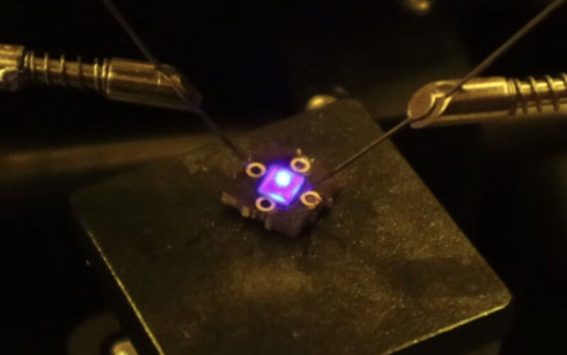
A YouTuber on a mission to liberate semiconductor manufacturing from the grip of multinational megacorporations is back with a new round of DIY success, this time manufacturing working LEDs in his backyard fab. Dr. Semiconductor, also known as semiconductor engineer Dr. Matthew Hartensveld, per his recently launched website, first caught the internet’s attention five months ago when he built a class-100 cleanroom in a shed in his backyard. Back in April, we wrote about his successful project to build his own DRAM in the clean shed, and the video he posted over the weekend on building his own LEDs follows that project with more ingenious success. Hartensveld’s decision to construct his own LEDs is directly connected to his RAMbitions, mind you - this isn’t some side project to light stuff up for fun. As Hartensveld notes in the video’s introduction, working DRAM cells are great, but they’re a far cry from functional DDR5 chips that can be plugged into a computer in lieu of ever-costlier chips from a major manufacturer. Turning cells into a RAM chip requires a lot more fabrication and packaging work, but there’s a problem there: attaching a finished silicon die to a circuit board requires lining up a whole bunch of tiny contacts with corresponding pads on the board. Because silicon is opaque to visible light, it takes more work to get everything aligned correctly. Enter LEDs made with gallium nitride (GaN): GaN is transparent, and LEDs still have to be attached to a circuit board to provide them with power, making them the perfect test bed for home packaging experimentation. “Not only does gallium nitride LED material help us develop our packaging process, it also helps us make some RGB,” Hartensveld said in the video. “And everyone knows RGB makes RAM faster … at least emotionally.” Etching GaN into LEDs traditionally requires the use of hazardous chlorine gases, which Hartensveld said in his video made it impractical and unsafe for his purposes - not to mention ridiculously expensive to either build or acquire the equipment necessary to do it safely. He instead decided to go with a laser etcher, using a 355 nm ultraviolet wavelength that GaN absorbs. After testing the laser etching process and finding it successful, Hartensveld moved on to a more traditional LED production flow, adding p-type contacts that supply positive charge and n-type contacts that supply negative charge using a typical process of applying photoresist and using metal deposition to fabricate his diodes. A bit of indium added to the etched GaN and supplied with power showed that the process worked, emitting the blue light expected from the InGaN quantum wells. From there, Hartensveld was able to add indium bumps to an ENIG-finished circuit board, which he used to attach the LED to the board. Because the LED itself is transparent, Hartensveld was able to show in the video how the indium contacts melted and formed a bond to the LED. Supplying power to the circuit board itself led to the same bluish light. Hartensveld also succeeded in changing the color of his LEDs to emit a warmer white light by covering them in the same yellowish material that is found covering the LEDs of most commercially available LED lightbulbs: Cerium-doped yttrium aluminum garnet. In other words, the project was a smashing success, not only for the democratization of LED manufacturing but also for his future efforts to build working RAM modules. “Going forward we can leverage our newfound packaging ability for RAM or really anything,” Hartensveld said in the video. He hasn't applied the new method to RAM module manufacturing yet, and while Hartensveld tells The Register he intends to do so soon, he has some additional work to do before he gets there. "The next step is shrinking both the transistor and, more importantly, the capacitor so I can increase the density and start experimenting with some of the techniques used in more modern commercial DRAM," Hartensveld said in an email. After shrinking comes scale, naturally. "As the features get smaller, alignment, process control, yield, interconnects and packaging all become much more difficult," The semiconductor doc added. "That's really what makes this interesting to me, figuring out how much of modern semiconductor fabrication can be reproduced with simpler, lower-cost equipment and processes." Chip democratization dreams While Hartensveld’s early work has been confined to a trio of YouTube videos, it appears he intends to go considerably further with his work. “Semiconductor fabrication is treated as something only billion-dollar fabs can do. It isn't,” he states in the about section of his website, semiconductor.diy. “A Class 100 cleanroom fits in a garden shed, sub-micron lithography can run on a modified microscope, and working devices can be made at home. This site documents how, openly, so anyone can build on it.” Hartensveld added in the video that he is working on open-source documentation for his entire process; bills of materials and instructions for his cleanroom shed and the LED project are already included on the site. The YouTuber also said that he’s planning to release videos on a more regular basis now that he has sponsorship from Vensa, a nonprofit backed by Ethereum cofounder Vitalik Buterin dedicated to the development of open-source silicon. “Microchips are the foundational technology for modern civilization, but making them is out of reach for most,” Vensa says of its project on its about page. “'Open Silicon' holds the most promise for democratizing chip design and improving the safety and sovereignty of computers.” LEDs made in a garden shed are just the first step. "I don't expect a shed fab to replace a billion-dollar commercial semiconductor fab, but I do think there is a huge unexplored space between 'you can design a chip' and 'you need access to an industrial foundry to actually make one,'" Hartensveld told us. He added that he hopes his work will give students, researchers, startups, and hobbyists the ability to experiment with semiconductor fabrication and make their own devices, making the process more accessible. "Democratizing semiconductor manufacturing and enabling a sort of small-scale or 'cottage' semiconductor ecosystem is definitely part of the vision," Hartensveld added. "The DRAM and LED projects are demonstrations of what's possible; now I want to keep shrinking the devices, improving the equipment and seeing how far this approach can actually be pushed." ®